Prototype Testing Details
Milky Way Systems has been ramping up testing as the PD150A differential probe design matures. This section provides more detail on testing our latest PD150A prototype, including test setups, test data, theory, and more.
Pulse response & rise time
This test shows PD150A’s response to a high speed pulse. The results verify the rise time specification and also allows checking for signal integrity issues such as overshoot or undershoot. The test was performed by applying a high speed differential pulse of about 2V peak-to-peak to the PD150A probe’s input. The probe’s output was monitored on a high speed oscilloscope with 1GHz analog bandwidth. The oscilloscope’s rise time measurement results showed a 10% to 90% rise time of 2.287ns. The orange markers show the 10% and 90% points used by the oscilloscope’s measurement.
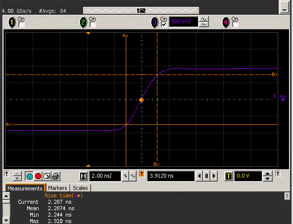
Close-up of probe output in response to a high speed differential pulse, with rise time measurement
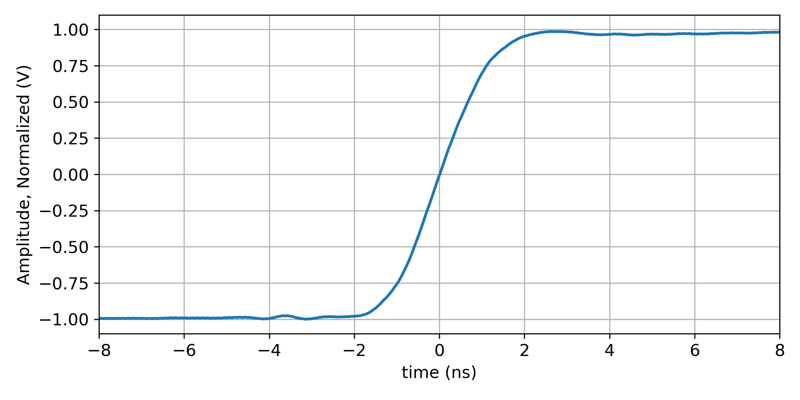
For a closer look at the probe output, the oscilloscope data is plotted below.
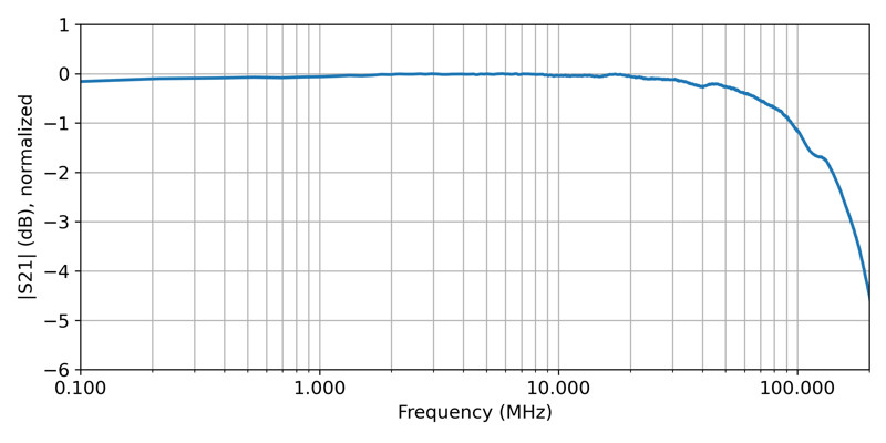
Frequency Response
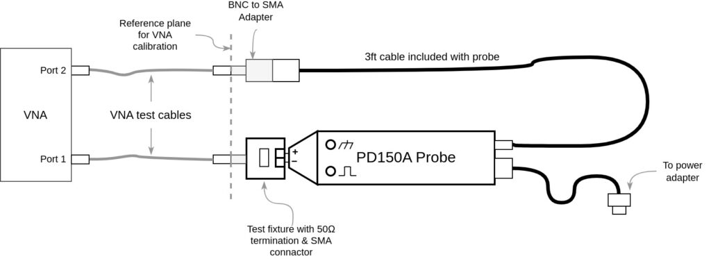
This section describes frequency response testing of the PD150A out to 200MHz. The results are used to quantify frequency response flatness and to verify bandwidth. The testing was performed in a 50Ω system. The measurements are performed using a Vector Network Analyzer (VNA). The VNA is outfitted with two coaxial test cables as shown in the diagram below, each with SMA connectors. The VNA is then calibrated at the output connectors of its cables as shown in the reference plane dotted line below. A special fixure is used to adapt the probe’s high impedance input to the test fixture. The fixture includes an SMA connector, a 50Ω termination, and two pins to connect to the probe input. The probe’s output is adapted to the setup with a BNC to SMA adapter.
The VNA in the above test setup was swept from 100 kHz to 200 MHz and S21 was recorded. The results were normalized to 0dB and plotted below.
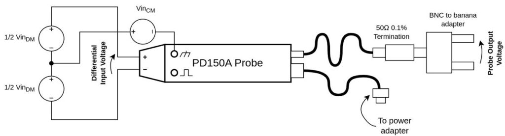
DC Differential Voltage Response
The following tests demonstrate the PD150A differential probe’s performance over a wide range of DC input voltages. The results validate the rated differential range of ±20V. They also show how PD150A behaves when exceeding the ±20V differential range.
All tests in this section use the setup shown below. On the left side of the setup are three adjustable power supplies which provide the probe’s input voltage. Two power supplies labelled 1/2 VinDM generate a differential input voltage. They are tracking power supplies, each contributing to one half of the full differential voltage. The third power supply, labelled VinCM, provides the common mode voltage. The right side of the diagram shows the probe’s output. The BNC side of the PD150A’s signal output cable is terminated with 50Ω precision inline terminator.
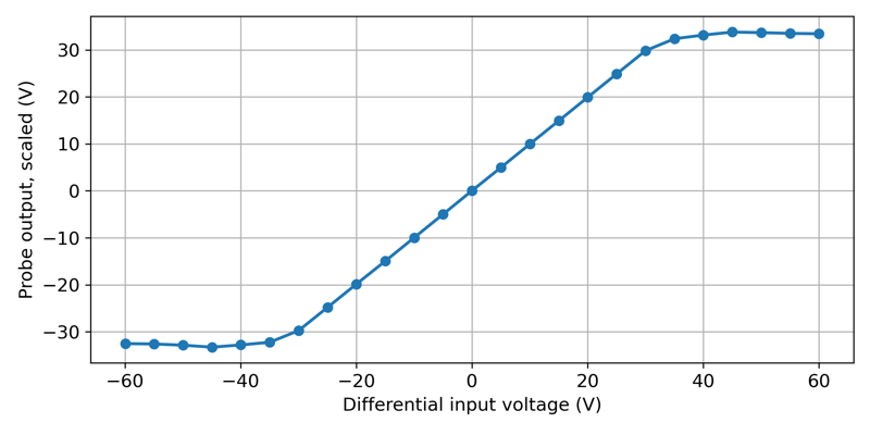
The first test shows the probe response to a purely differential DC voltage, which was generated using the two power supplies labelled 1/2 VinDM in the above diagram. For this test, the VinCM power supply was set to 0V, keeping the common mode voltage equal to 0V. The differential voltage was swept in small increments from -60V to +60V. At each step, the differential probe input voltage and the probe output voltage was measured. The resulting response is plotted below. On the horizontal axis is the differential voltage applied to the probe input. The vertical axis shows the probe output times twenty, to account for the probe’s 20:1 attenuation. The plot shows the probe output closely tracking the differential input voltage within its ±20V specification. Beyond ±20V, the probe output begins to saturate, causing the plot to flatten.