PD150A
150MHz Differential Probe – In Development
Highlights | Design | Specifications | Performance Plots | Detailed Testing | Availability
PD150A differential probe at a Glance
PD150A is a compact 150MHz differential probe optimized for reliable measurement at reasonable cost. Its small probe tip lets you probe close to sensitive or high frequency circuits for consistent results. PD150A’s automated tuning features make it easy to maintain optimal performance.
PD150A turns an oscilloscope into a differential measurement tool, allowing you to measure non ground referenced voltages in power converters, differential digital and analog interfaces, and many other circuits. It is also helpful for measuring ground referenced voltages which are corrupted by ground noise.
PD150A is under development. See below for a detailed description, specifications, and more.
Features & Performance Highlights
- 150MHz 3dB bandwidth
- 20:1 Attenuation
- Differential range of +/-20V with up to +/-30V common mode
- Input sockets with 0.1in (2.54 mm) spacing
- Several probe accessories
- Very low input capacitance minimizes circuit loading (<3pF differential)
- Probe inputs protected to +/-100V from oscilloscope ground
- Automated DC bias and common mode rejection ratio tuning
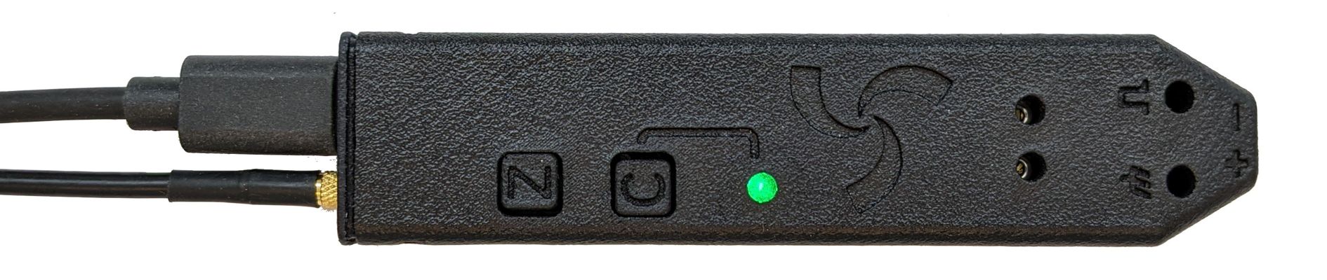
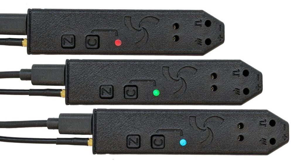
- LED oscilloscope channel indicator
- Compatible with most oscilloscopes
- 3ft (91cm) signal output cable
- USB power connection via USB-C connector (5V nominal)
Design & Features
Versatile Probing
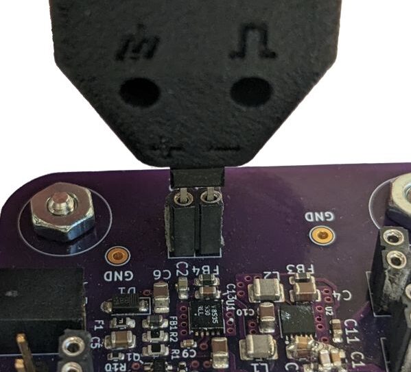
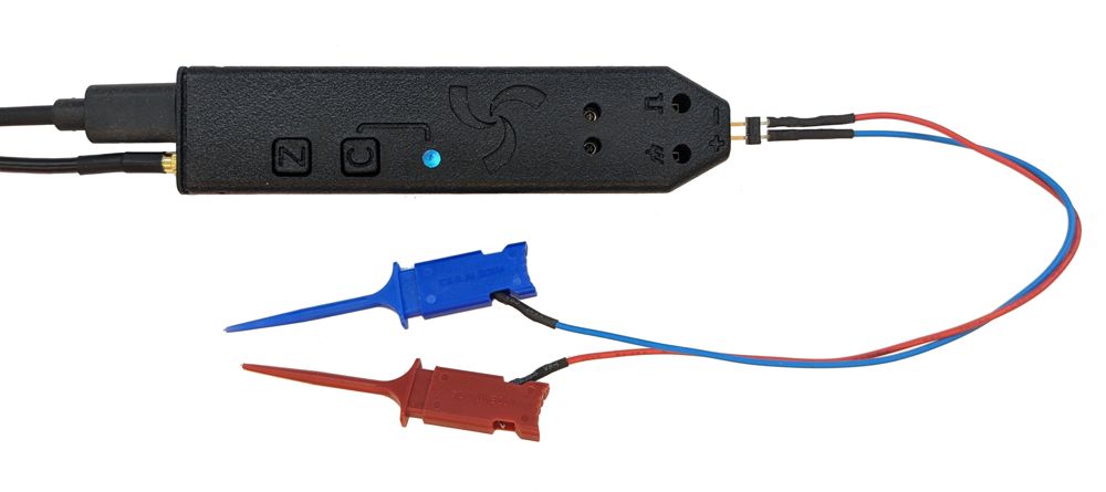
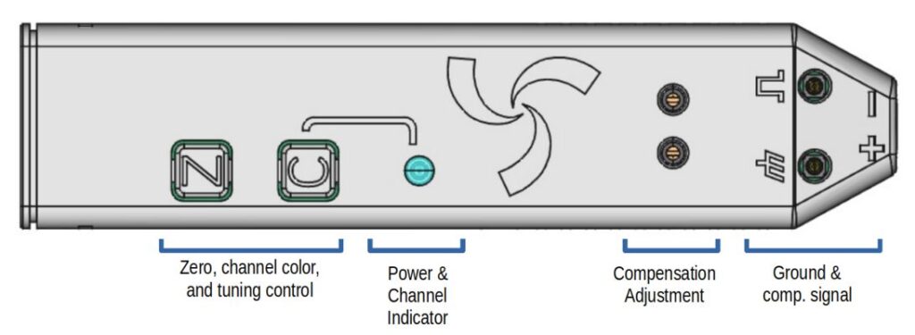
PD150A has two input sockets on the front of the probe spaced 0.1 in (2.54 mm) apart. When you need optimal performance, connect the sockets to a two pin header soldered into the circuit under test. The close connection minimizes parasitic capacitance, lead inductance, and field coupling. Therefore, you can be assured of reliable results when probing high frequency or sensitive signals.
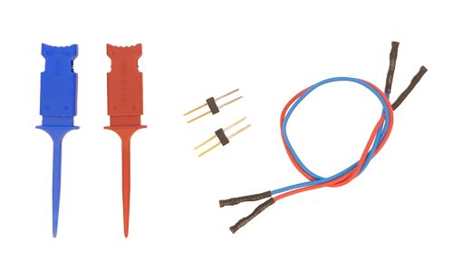
When probing less critical signals, the inputs do not have to be placed so close to circuit under test. Instead, place the probe farther from the circuit and connect its inputs with jumper wires. To do so, simply attach jumper wires into the input sockets. For example, use a male-female jumper wire to connect the probe inputs to a standard 0.1 in header, or to a pair of mini-grabbers
USB Power
PD150A has a USB Type-C power connector. Power it with the included adapter or with another USB port or power source. It is compatible with compliant USB Type-C adapters and with most ports with Type-A receptacles. When using a Type-A port for power, use a USB Type-A to USB Type-C cable (included). Note that the USB port must support 5V and at least 300mA.
Compatibility
PD150 is compatible with most oscilloscopes. For oscilloscopes with a 50Ω input rated for at least 2.5Vrms , connect the BNC end of PD150’s coaxial cable directly to the input. Alternatively, PD150A may be used with a high impedance oscilloscope input. To do so, place a 50Ω inline attenuator (not included) between the oscilloscope input and the BNC connector on PD150A’s coaxial cable.
Keep Track of you scope channels
PD150A’s power LED doubles as an oscilloscope channel indicator. Simply press the “C” button to cycle through several colors.
Attention to detail
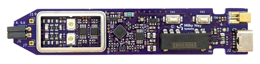
PD150A’s sensitive components are shielded within an EMI enclosure for reliable performance in noisy environments. The signal and power cables are replaceable and attach through connectors. PD150A’s design avoids low reliability components such as potentiometers or electrolytic capacitors.
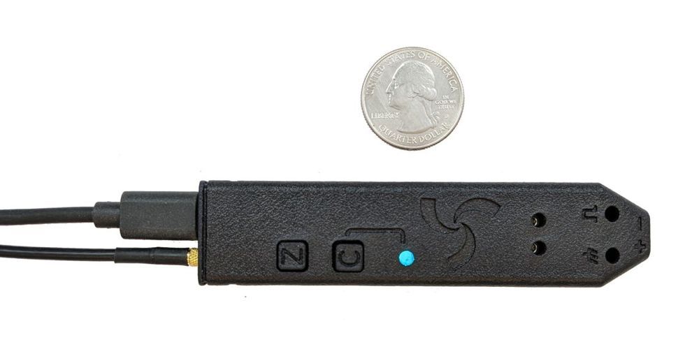
Compact size
PD150A packs a lot of features and performance into a small volume, measuring 10 x 2.4 x 1.5 cm.
Automated DC offset Adjustment
Fine tune PD150A’s DC offset by disconnecting the probe input and pressing the “Z” button. This will automatically tune the probe’s DC performance, ensuring that a 0V input produces a near 0V output.
Automated low frequency common mode rejection adjustment
A perfect differential probe would reject a common mode voltage applied to its inputs. In other words, it would produce a zero output when applying the same voltage to each input. However, differential probes always exhibit some output under this condition. This non-ideal behavior is caused by slight imbalances in the probe’s circuitry, which can be minimized by periodic adjustment.
Adjusting common mode rejection is a tedious process on many probes, often requiring external test equipment and careful tuning. PD150A reduces this process to a couple minutes, thanks to its automated adjustment.
To learn more about common mode rejection and how it is characterized, see Wikipedia’s page on Common Mode Rejection Ratio.
Easy to access compensation adjustment
PD150A has frequency compensation capacitors for both inputs. Both are accessible through openings on the top of the probe. Adjust these for optimal gain flatness and high frequency common mode rejection. PD150A’s built-in compensation signal provides a flat square wave output with sufficient rise time to help with consistent adjustment.
Minimal circuit loading
PD150A has a high impedance input to minimize its effect on the circuit under test.
What’s included
PD150A comes with a variety of accessories to support your testing needs.
- PD150A Differential Probe
- USB Power Adapter
- USB Power cable
- Coaxial Signal Cable (3ft)
- Jumper cables (2x)
- MIni-grabbers (2x)
- Dual-pin headers (2x)
Specifications & Characteristics
Characteristics:
- 20:1 Attenuation
- 50Ω output impedance
- USB power connection via USB-C connector (5V nominal)
- Input sockets with 0.1in (2.54 mm) spacing
- Automated DC offset adjustment
- Semi-automated low-frequency CMRR adjustment
- Manual compensation adjustment
Specifications:
| Differential signal range | ± 20V |
| Common mode range | ± 30V |
| DC offset voltage | ≤ ± 10mV, referenced to input, after performing zero adjustment |
| CMRR, 60Hz | ≥ 70dB, referenced to input |
| CMRR, 10MHz | ≥ 40dB, referenced to input |
| Input Resistance, between inputs | 1.08 MΩ between inputs, 540 kΩ from each input to ground, typical |
| Input Capacitance at 10kHz | ≤ 3 pF between inputs, ≤ 6 pF from each input to ground, typical |
| DC Attenuation Accuracy | ≤ ± 5% |
| Pulse Rise Time (10% to 90%) | ≤ 2.4 ns |
| Gain Flatness, 0-30MHz | ≤ ± 0.5dB , typical |
| Input Damage Threshold | 100 V |
| Bandwidth, 3dB | ≥150 MHz |
Typical Performance Plots
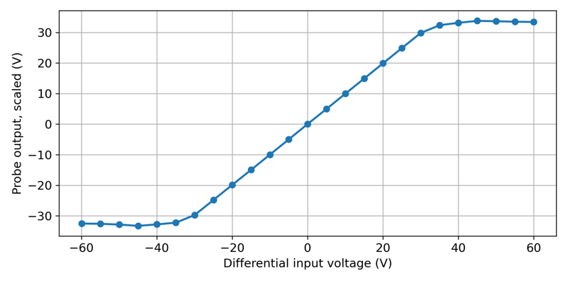
This plot shows PD150A’s response to a DC differential input voltage ranging from -60V to +60V. Note the linear response when operating within its ±20V specification.
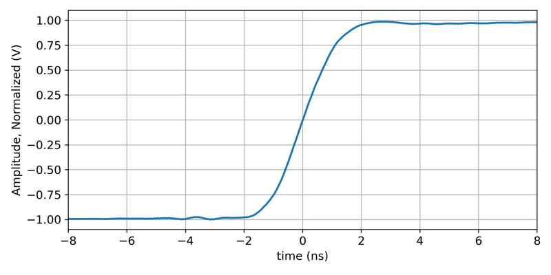
PD150A’s response to a differential pulse is shown below. For this test, a high speed differential pulse with an amplitude of approximately 2V peak to peak was applied to the probe input.
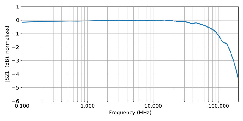
The following plot shows PD150A’s typical frequency response. The measurement was made with the probe input connected to a single-ended 50Ω system.
Availability
PD150A is in late prototype stage. To learn more, see the detailed testing page.